
Specifications:
| Material | InAs single crystal | Orientation | <100> |
| Crystal Structure | Cube | Density | 5.66g/cm3 |
| Melt Point | 942℃ | Bandgap(@300 K) | 0.45eV |
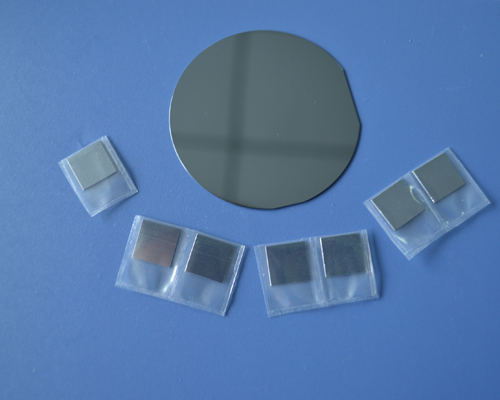
| Size(mm) | 10x10x0.5mm, 5x5x0.5mm, D50.8x0.5mm, D76.2x0.5mm |
Surface Roughness | Ra≤5Å |
| Polishing | SSP (single surface polished) or DSP (double surface polished) |
Package | class 1000 clean room, class 100 bags |
Chemical Properties of InAs Crystal:
| Single Crystal | Doping | Conduction Type | Carrier Concentration | Mobility Ratio | Dislocation Density |
| InAs | / | N | 5x10¹⁶ | 2x10⁴ | <5x10⁴ |
| InAs | Sn | N | (5-20)x1017 | >2000 | <5x10⁴ |
| InAs | Zn | P | (1-20)x1017 | 100-300 | <5x10⁴ |
| InAs | S | N | (1-10)x1017 | >2000 | <5x10⁴ |
Indium Arsenide (InAs) single crystal is often used as the substrate material to grow heterojunction materials (InAsSb/In-AsPSb, InNAsSb), which can be utilized to manufacture infrared-emitting devices within the wavelength range 2~14μm. Indium Arsenide (InAs) can also be used as a substrate material for the epitaxial growth of AlGaSb with a superlattice structure for medium wave infrared quantum cascade laser(QCL). InAs are widely used in gas monitoring and low-loss optical fiber communication. With a high mobility ratio, it is an ideal material for Hall semiconductors. As a single-crystal substrate, Indium Arsenide has low dislocation density, good lattice integrity, appropriate electrical parameters, and high homogeneity. The main growth method of this material is the classical liquid encapsulation pulling method (LEC).
Shanghai North Optics offers custom Indium Arsenide substrate and wafers according to the request, with a good surface roughness of less than 0.5nm and packaged in class 1000 clean room and class 100 bags.
Copyright © 2012-2024 All Rights Reserved. 京ICP备01000000号 XML