
| Material | GaSb single crystal | Orientation | <100> |
| Crystal Structure | Cube | Density | 5.53g/cm3 |
| Melt Point | 712℃ | Bandgap(@300 K) | 0.67eV |
| Size(mm) | 10x10x0.5mm, 5x5x0.5mm, D50.8x0.5mm, D76.2x0.5mm |
Surface Roughness | Ra≤0.5nm |
| Polishing | SSP (single surface polished) or DSP (double surface polished) |
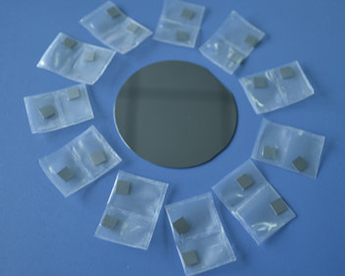
Package | class 1000 clean room, class 100 bags |
Chemical Properties of GaSb Crystal:
| Single Crystal | Doping | Conduction Type | Carrier Concentration | Mobility Ratio | Dislocation Density |
| GaSb | / | P | (1-2)×1017 | 600-700 | <1x10⁴ |
| GaSb | Zn | P | (5-100)x1017 | 200-500 | <1x10⁴ |
| GaSb | Te | N | (1-20)x1017 | 2000-3500 | <1x10⁴ |
Gallium Antimonide (GaAs) is used as a substrate material for the epitaxial growth of heterostructures, which are harnessed for optoelectronic applications. The lattice constant of GaSb matches well with various ternary, quaternary, and III-V compound solid solutions whose bandgap covers 0.8–4.3 μm, which makes it a good substrate material used in infrared optical fiber transmission. With higher lattice-restricted mobility than GaAs, GaSb is expected to have good prospects in the field of microwave.
Shanghai North Optics offers custom GaSb crystals and substrates according to the customer’s request, the maximum diameter of 3” is available. Three types of GaSb materials: non-doping, Zinc (Zn) doped and Tellurium (Te) doped GaSb are offered. All substrates are stringently tested and packed in class 1000 clean room and class 100 bags.
Copyright © 2012-2024 All Rights Reserved. 京ICP备01000000号 XML