
| Code | Size | Thickness | Orientation | Surface Finish | Unit Price | Delivery | Cart |
|---|---|---|---|---|---|---|---|
| 645-001 | 5x5mm | 0.5mm | <100> | SSP | Inquire | 2 weeks | |
| 645-002 | 5x5mm | 0.5mm | <100> | DSP | Inquire | 2 weeks | |
| 645-004 | 5x5mm | 0.5mm | <111> | SSP | Inquire | 2 weeks | |
| 645-005 | 10x10mm | 0.5mm | <100> | SSP | Inquire | 2 weeks | |
| 645-006 | 10x10mm | 0.5mm | <100> | DSP | Inquire | 2 weeks | |
| 645-007 | 10x10mm | 0.5mm | <110> | SSP | Inquire | 2 weeks | |
| 645-008 | 10x10mm | 0.5mm | <111> | SSP | Inquire | 2 weeks | |
| 645-009 | φ25.4mm | 0.5mm | <100> | SSP | Inquire | 2 weeks | |
| 645-010 | φ25.4mm | 0.5mm | <100> | DSP | Inquire | 2 weeks | |
| 645-011 | Φ50.8mm | 0.5mm | <100> | SSP | Inquire | 2 weeks | |
| 645-012 | Φ50.8mm | 0.5mm | <100> | DSP | Inquire | 2 weeks | |
| 645-013 | Φ76.2mm | 0.5mm | <100> | SSP | Inquire | Inquire | |
| 645-014 | Φ76.2mm | 0.5mm | <100> | DSP | Inquire | Inquire |
LaAlO3 (Lanthanum aluminate) single crystal with a perovskite crystal structure, has a good lattice match to multiple materials with a similar perovskite structure. Its wide bandgap, thermal stabilities, and low dielectric loss make it excellent for applications in electronics of high frequencies, optics, and indispensable platforms for the epitaxial growth and research of thin films and heterostructures. Various materials can be grown on LaAlO2, including complex oxides, high-temperature superconductors, magnetic materials, and multiferroics. LaAlO3 exhibits a high dielectric constant, making it useful in capacitor applications.
Shanghai North Optics provides stock epi-ready LaAlO3 wafers and custom LaAlO3 wafers upon request.
Applications of LaAlO3 Substrates:
Epitaxial Growth: LaAlO3 substrates serve as templates for the epitaxial growth of complex oxide thin films, including high-temperature superconductors, magnetic materials, and multiferroics. The lattice match between LaAlO3 and the deposited material enables the precise control of film quality and interface properties.
Electronics: In electronics, LaAlO3 substrates find applications in the fabrication of high-performance field-effect transistors (FETs), resistive random-access memory (RRAM), and photonic devices. The compatibility of LaAlO3 with various deposition techniques allows for the integration of diverse functional materials and device architectures.
Optoelectronics: LaAlO3 substrates play a crucial role in the development of optoelectronic devices such as light-emitting diodes (LEDs), photodetectors, and electro-optic modulators. The transparent nature of LaAlO3 in the visible and near-infrared spectrum makes it suitable for optical applications.
Fuel Cells and Sensors: LaAlO3-based thin films are investigated for applications in solid oxide fuel cells (SOFCs), gas sensors, and catalysis. The high chemical stability and ionic conductivity of LaAlO3 facilitate efficient ion transport and electrode performance.
Common Specifications:
| Material | LaAlO3 crystals | Orientation | <100>,<110>,<111> |
| Orientation Error | ±0.5° | Maximum Diameter | 3 inches |
| Typical Thickness | 0.5mm, 1.0mm | Thickness Tolerance | ±0.05mm |
| Size Tolerance | ±0.1mm | Surface Finish | SSP or DSP |
| Roughness | Ra<0.5nm | Cleanness and Package | class 1000 clean room, class 100 bags |
Curves:
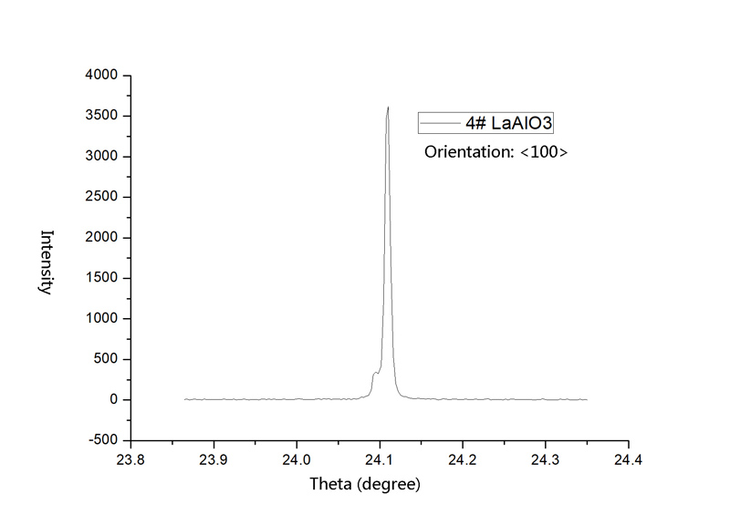
1)Typical X-Ray Diffraction (XRD) Curve of LaAlO3 <100> Crystals Substrates
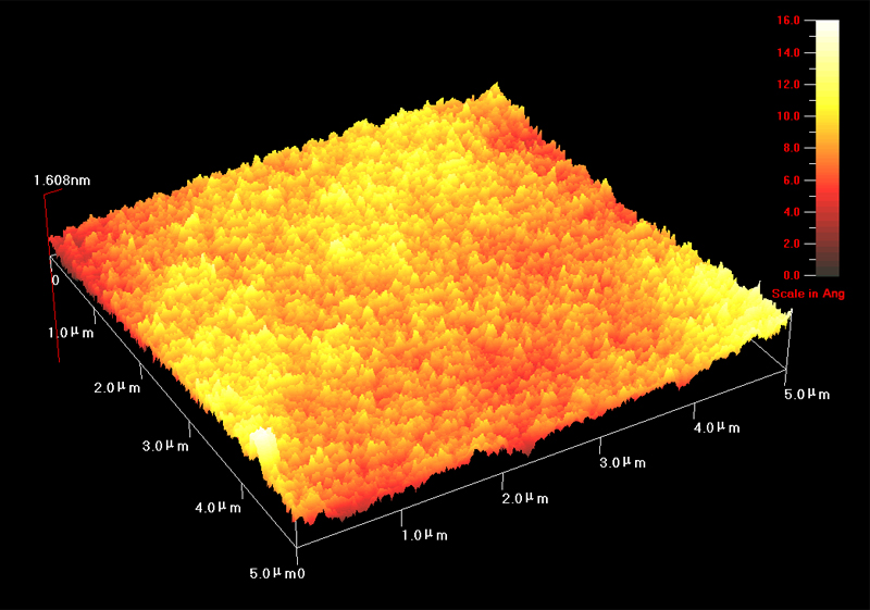
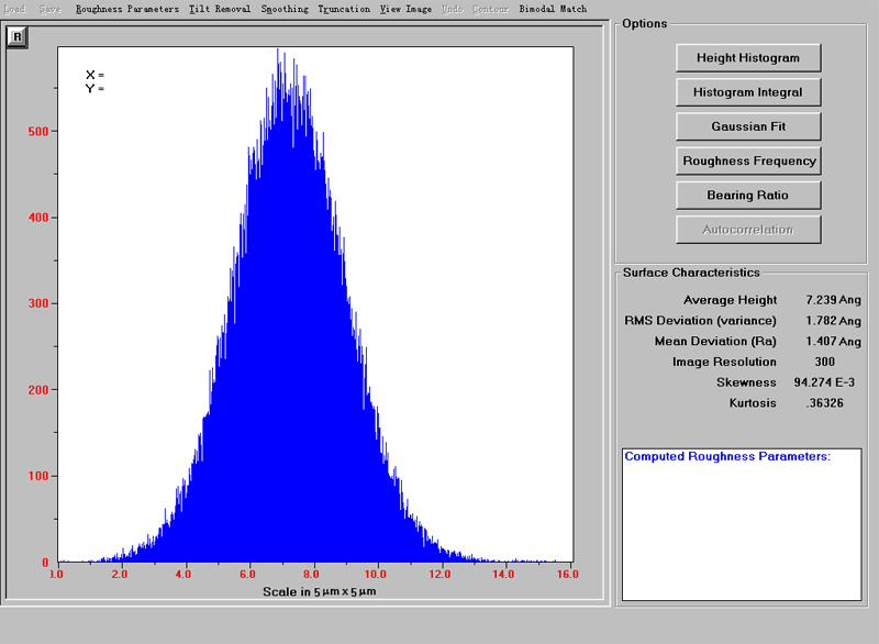
2) Typical Surface Roughness of substrate LaAlO3 <100> and <001> measured by Atomic Force Microscope (AFM) in 5μm x 5μm Scale

Copyright © 2012-2024 All Rights Reserved. 京ICP备01000000号 XML